
In today’s lab experiment I revisit the topic of application-specific integrated circuits (ASIC) with Field Programmable Gate Arrays (FPGAs). These high-speed and flexible computing fabrics allow for processing in which the datapath and control flow is specified and is optimal for its intended purpose. This is of course advantageous in systems that require fast and computationally intensive processing of large amounts of data (such as a high-speed nano-scale microscope) in comparison to general microprocessors which are limited by the fetch-execute cycle.
I wanted to revisit this topic because of its applications into Self-Reconfigurable Computer Architectures which are mainly characterized by a hardware/software codesign of a microprocessor with FPGA fabric. The principle of this type of architecture is to capitalize on combining some flexibility of software with high performance special purpose processing by way of “loading” a new circuit as needed during runtime.
However, as a preliminary segue into learning about Reconfigurable Computing, I started by implementing a custom circuit design in hardware description language (HDL) to be simulated and synthesized for execution. The intention of this is to later explore the software architecture and how they’re integrated in application specific reconfigurable systems.
The circuit to be implemented will generate a certain count (that changes every 0.5 seconds) depending on the value of the input x (i.e., x = 0: 0,1,2, 4, 8,0,1,… x = 1: 0,5,7,11,13,0,5,…). However the count will change sequence only when the current sequence is completed. An enable signal E will also allow the count to pause or continue. The I/O for this includes a reset (active high), E (enable), x (control), and clock, and an output of a single 4-bit signal which represents the count value.
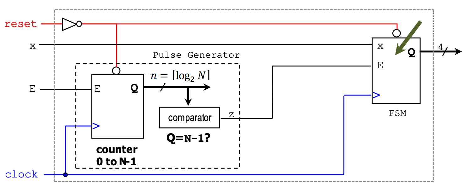
The design to meet this purpose turns out to be relatively simple and essentially has only two main components: 1). A counter modulo-N that is driven by the system clock and generates a 1-cycle pulse every N cycles and 2). A finite state machine (FSM). The output from the pulse generator is fed to the input of the FSM. The descriptive behavior of the FSM component will end up looking something like this:
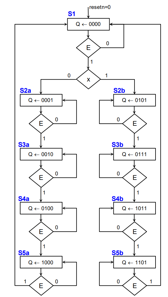
The result of this logic is also fairly straightforward in which the state and final output Q is determined by x and the enable signal E is driven synchronously by the signal from the pulse generator. Here the input signal of x is only considered at the start of a new sequence. Thus If x changes, the count sequence is altered only after the current sequence is completed. The FSM remains in the same state as E (signal z from pulse generator) = 0 and continues when E=1.
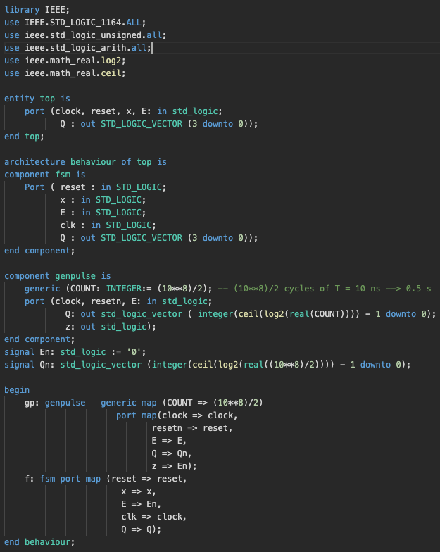
The datapath and control flow of this circuit was implemented with VHDL in Vivado 2019.1. The pulse generator can described in this way:
Pulse Generator
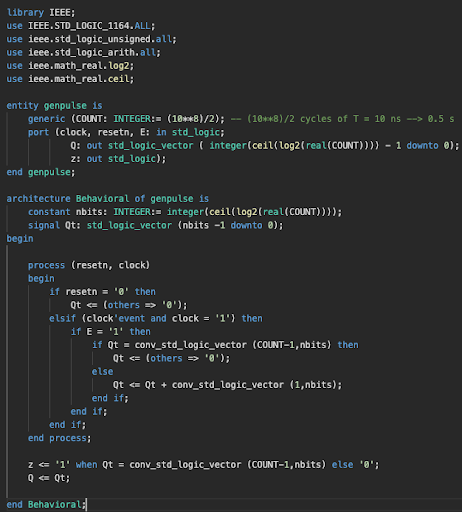
Here we take a generic count variable which will determine how many cycles of our input clock period we’ll need to achieve a pulse of 0.5 seconds. This will specify our modulo-N counter with nbits, generating the pulse and resetting when our internal signal Qt = 2N-1.
The Pulse Generator and FSM are then instantiated in a Top File and port mapped to describe how the components are connected with the the high-level I/O and variables defined, as follows:
Top File
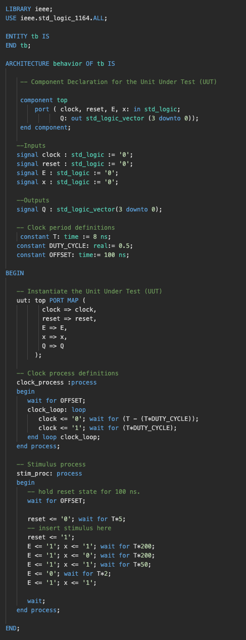
After the hardware has been specified, it’s time to simulate how the circuit will function. This was done with a testbench file to emulate the input signals into the circuit:
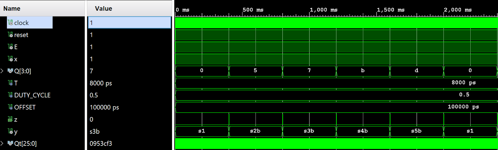
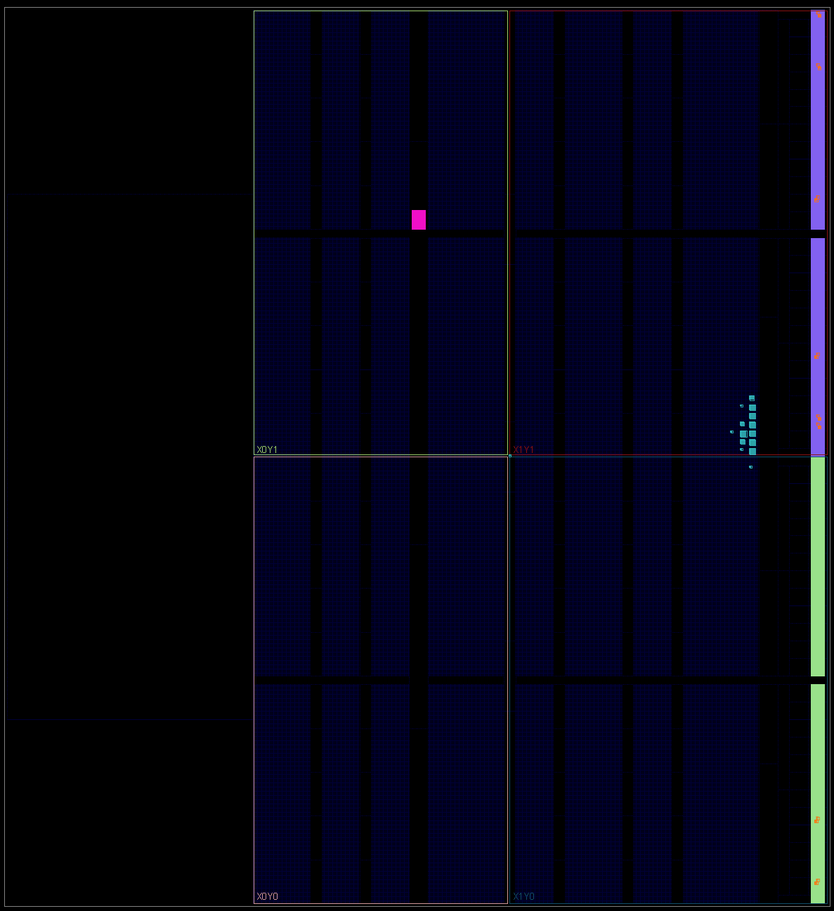
The resulting simulation shows the four bit output Q in each state y with given input x and pulse generator signal z as enable to control the count output every 0.5 seconds:
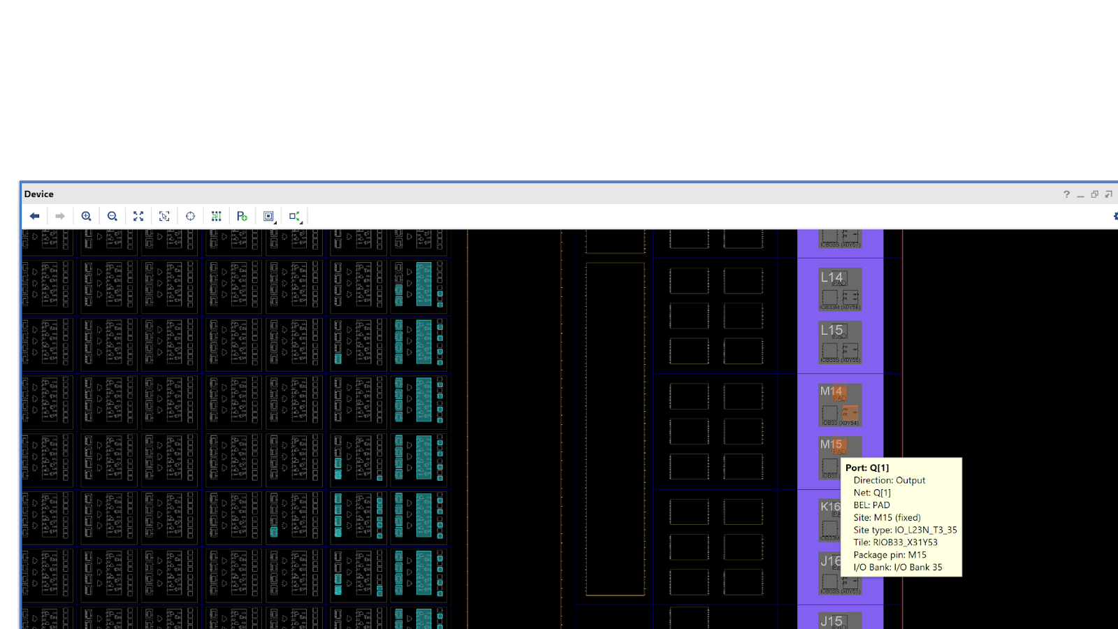
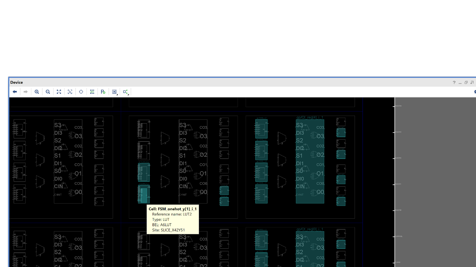
We can also synthesize this circuit and visualize how the logic will be physically placed on the intended board of interest by defining constraints which map the user defined I/O signals to the board’s specified architecture. Located on the right hand side of this map are the input and output signals (clock, reset, x, E, and Q, highlighted in orange), and the synthesized circuit is highlighted in blue (gen pulse and FSM).
The next step would be to generate the bitstream that would be loaded onto the FPGA board where we’d be able to visualize the counter on I/O such as LEDs and switches. Given that I did not have an FPGA board to do this, I was at least able to complete the extent of what can be done with the confidence that it will behave as intended. This experiment in total only took a few hours including a lengthy Vivado install and getting reacquainted with VHDL syntax and project structure.
This circuit is not necessarily interesting on its own but the goal is to hopefully do several more iterations of this process with more complex processing requirements, introduce co-processing with software on a microprocessor with tools and profiling, and ultimately build an application-specific reconfigurable system.